The Next Generation of Computation - where will it take us?
Graphcore. A new and novel start-up company, on a mission to develop an entirely new processor, with the goal of accelerating the growth of innovations in the fields of Artificial Intelligence (AI), and much more.
This article is a reiteration of a talk presented by Simon Knowles, the CTO and co-founder of Graphcore, at the RAAIS Conference in London, 2017, of which you can find here / here
There are two major processing components in a computer that executes all computational processes. The Central Processing Unit, and the Graphics Processing Unit.
While the CPU is designed to execute instructions provided by a computer program, to achieve a certain operation or output, and a GPU is designed to efficiently ‘manipulate and alter memory to accelerate the creation of images’, Graphcore’s Intelligence Processing Unit (IPU) is instead designed, to process what are known as Graphs, which is the primary mode of expression for understanding, implementing and evolving Machine Learning in computational systems.
Simon Knowles describes the IPU as follows, “An IPU-style machine is a pure, distributed, parallel processor.” It is designed so that, “we can build little ones, big ones, and in the future, really, really big ones, and it will still be the same machine.”
Let’s break down what this means.
-
First, the IPU is ‘pure’, meaning it is designed purely for Artificial Intelligence applications. The IPU does not deal with any graphics or High-Performance Computing (HPC) applications like GPU’s, and is designed purely for Machine Learning purposes. It is a “Memory-Centric power device”.
-
Second, the IPU is distributed. In other words, the IPU holds thousands of little localised processor and memory modules that all process and exchange information (We will elaborate on this characteristic below.)
-
Third, the IPU is parallel, meaning all those little processing units compute parts of the program simultaneously. Once complete, they all exchange messages before repeating the cycle (see Bulk Synchronous Parallel, below.)
-
Finally, the IPU’s design characteristics make it readily scalable into very large systems in the near future.
Next, let’s delve deeper into the IPU’s architecture, and discover the motivations behind its design.
Under the hood, the IPU consists entirely of many independent little processors, with their own localised memory, that can send messages to each other through what Simon calls, “a completely stateless, perfect interconnect”. This means that nothing in the IPU is shared, which makes for HUGE parallelism. “There is no shared scheduler, as scheduling is achieved by the compiler” - as opposed to scheduling directly in the processing unit, which is what occurs in a CPU and GPU - “and there is no shared memory, because this would limit scalability.”
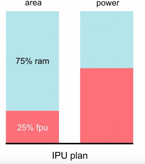
Figure 1: As you can see, the IPU comprises of two parts. The Random-Access-Memory (RAM), where information is stored and retrieved, and the Floating-Point-Unit (FPU), where arithmetic operations take place on the data. Remember, both memory and processor are distributed (see Figure 2)
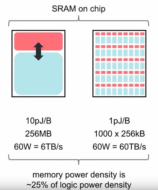
Figure 2: The IPU is formatted akin to the profile on the right of this figure. There are thousands of very small, processors coupled with memory modules.
Why design a processor in this fashion?
The IPU is designed with a different motivation to the CPUs and GPUs currently on the market. The objective for the IPU is to harness as much of its available power as possible, instead of “using all the stuff on your chip, at the same time, and as much as possible.”
The goal is to achieve as much bandwidth for the same power budget as today’s GPU’s.
“Could you deal with models which lived entirely on the chip, that had less memory available to them, but that memory was far more accessible to the arithmetic, for the same power budget?”
Well, this is perfect for Machine Intelligence applications - higher compute for the same power usage. Fantastic!
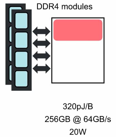
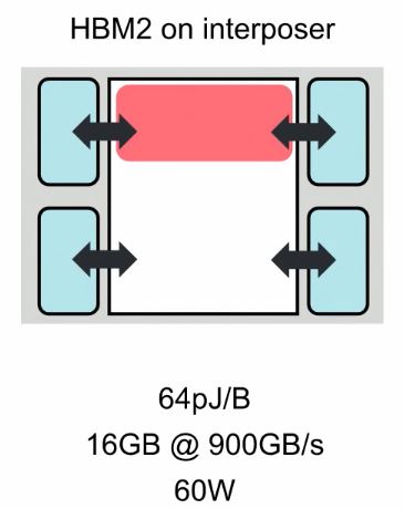
Figure 3: Left - External Synchronous-Dynamic-Random-Access-Memory cards working for a CPU; Right - A recently innovation for external memory to a GPU, known as High-Bandwidth Memory (HMB).
As you can see in Figure 3, both solutions involve memory outside of the processing unit. Some of the performance limiters in Machine Intelligence processing, are:
- Rate of arithmetic
- Bandwidth / Latency of data access
- Rate of address calculation
However, the biggest limiter of them all is POWER. This is why the IPU is designed the way it is. To make full utilisation of all power available to it, in order to make the most of achieving its purpose.
Why is power a limiting factor?
Power limits all digital silicon today, and so, we must make the most of the power we can harness from the utilisation of this material in our electronic devices. There is in fact an upper limit for power you can get out of a silicon chip, and secondly, there is a limit to the size at which we can manufacture a silicon chip.
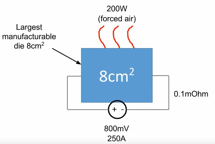
Figure 4: The upper limit for the manufacturing of a chip is approximately 8 squared-centimeters. This can hold up to about 25 million transistors, and can be fed up to about 200W of power.
Compared with the IPU, GPU’s tend not to make full use of their available power for Machine Learning applications, and therefore there is room for improvement in processor design for this particular purpose.
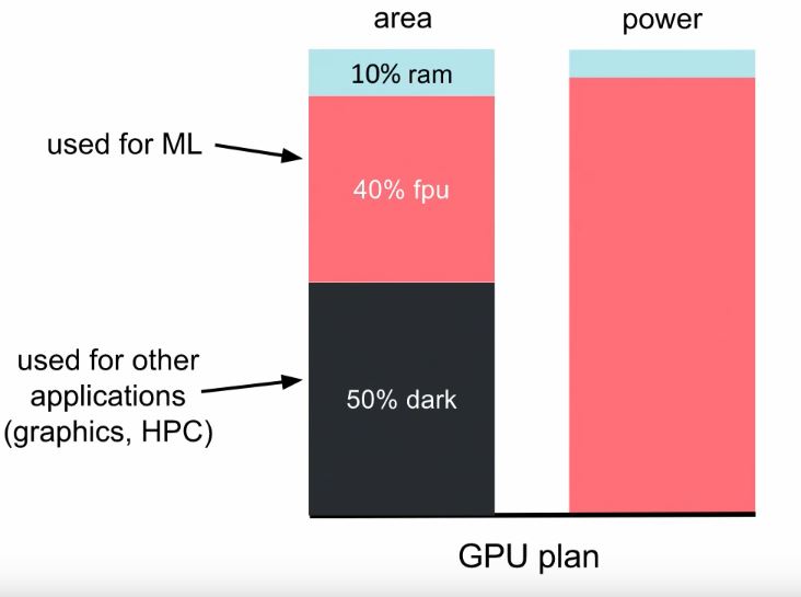
Figure 5: The dark area is what engineers call ‘Dark Silicon’. Dark Silicon describes the wiki ‘amount of circuitry that cannot be powered-on at the nominal operating voltage for a given thermal design power (TDP) constraint’, and this results from the failure of what is called Dennard Scaling, a phenomenon whereby, as transistors become smaller, their power density remains constant, ‘so that the power use stays in proportion with area’.
So, up to this point, we have learnt that due to the limitations on the use of Silicon in our electronic devices, we must utilise all of the available power and that a distributed memory-processor design is optimal to enable high performance, Graph-based computation, for Machine Learning applications.
With this in mind, for maximum silicon efficiency, we also need to operate with serial communication and compute. You are probably thinking, “Wait!, I thought we wanted a parallel system for maximum throughput…”. Here’s why.
When the distributed system works in parallel, it is executing arithmetic at the same time as exchanging information between processes in the system. This is not full utilisation of all available power. Instead, we want to operate our distributed system in serial. This way, all available power is used first for the compute phase, and once completed, all available power is used for the exchange phase. So, how is this better?
As Simon puts it, “We get to use all of the power available, and we get the answer to our program, earlier!”. So, as shown in Figure 6, below, for the same power budget, instead of saving power and operating below 100%, we save time!
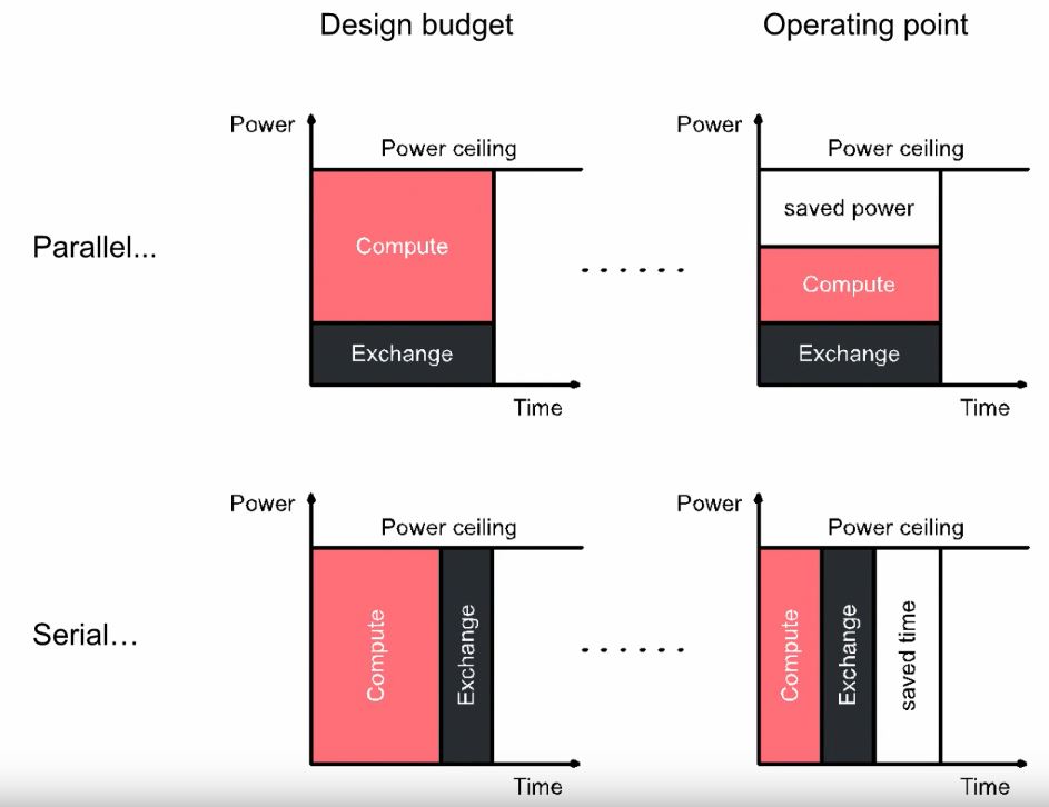
Figure 6: Comparison between parallel and serial communications in relation to the power consumed and the time of operation.
But, there IS a catch… In order to operate a distributed system in serial, all our little processors must have a collective reference on time, so each of them knows where each other is in their programs.
This is where ‘Bulk Synchronous Parallel’ (BSP) computation comes into play.
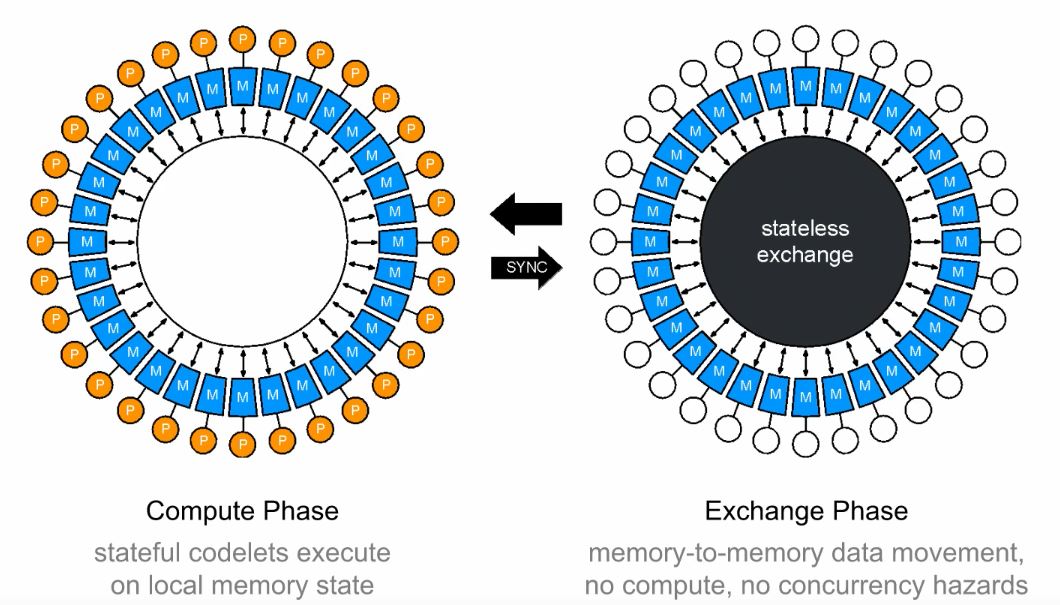
Figure 7: A depiction of the BSP process
The idea of this computational mechanism is to alternate between localised, distributed computation and collective exchange of messages between memories.
The first stage of a BSP-driven computation is for all the processors to run their computations on their own local memory. Once all processors agree that they have finished computing, they all synchronise and move onto the communications phase of this process, called the Exchange phase, where messages are exchanged between processors’ memory modules. Once complete, this two-stage procedure repeats.
This solution enables seamless communication between processors in the exchange phase, known as non-blocking communication, which means that any given process does not have to wait for any event in the computer system to execute. In other words, a process does not block the execution of another, saving time and maximising power usage.
Non-blocking communication cannot be achieved with today’s conventional processor architectures.
In the past, BSP was not a popular solution, since there was no such chip like the IPU and all processing units accessed their memories external to the chip. In this case, there are two major disadvantages to BSP:
- Synchronisation off-chip is very expensive in terms of power usage and design, and it takes a long time to complete synchronisation.
- The bandwidth required off-chip is also very expensive.
So, looking at the overall picture we see that there is a trade-off between two variables, memory and compute.
IPU memory > GPU memory
IPU compute < GPU compute
To conclude this article, we are going to see how Graphcore’s IPU closes the gap between a Multi-Giga-Byte GPU system with external memory and lower compute & an IPU system that only has a fraction of a Giga-Byte on the chip, but very high compute capabilities.
First, we must introduce some terminology.
Deep Neural Network - a neural network with a certain level of complexity, a neural network with more than two layers. Deep neural networks use sophisticated mathematical modeling to process data in complex ways.
Graph - A discrete mathematical structure, or network, comprising of a set of objects (known as vertices or nodes) which are in some way connected by what are called edges or links.
Vertex / Node - A fundamental unit of a Graph in discrete mathematics.
Edge / Link - A mathematical unit represented graphically as a line, which can either be directed or undirected.
Activation function - A function associated with a vertex, that defines the output of that vertex when given an input or set of inputs.
Gradient Descent - An optimization algorithm used to minimize some function by iteratively moving in the direction of steepest descent as defined by the negative of the gradient. (Used to update weights).
Weight - A foundational concept in artificial neural networks. In artificial neural networks, vertex’s input equals the sum of weighted outputs from all neurons in the previous layer.
With these definitions in our arsenal, what then determines the state in the IPU?
- Graph connectivity (model structure)
- Vertex code (model behaviour)
- Persistent data (model parameters)
- Ephemeral data (model activation) Ephemeral data refers to a data structure that never preserves the previous version of itself when it is modified.
So now, looking at the diagrams below in Figure 8, how do we optimise our algorithm to account for the limited compute capabilities of the IPU?
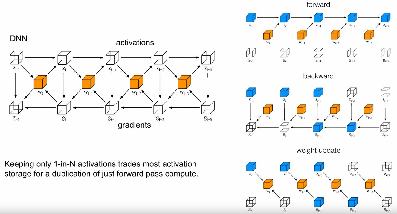
Figure 8: Left - A chunk of a Deep Neural Network (DNN), comprising of a series of activations on the top, a series of gradients on the bottom, and a series of weights in the middle. In training the DNN, you sweep along the activations up top, then sweep along the gradient below.
NOTE: I am still yet to fully understand the mechanism of the DNN algorithm demonstrated above. For the more experienced reader, here is Simon’s explanation from the talk:
“In a scenario where you want to minimise computation, save all forward activations. You’ll require them when you go backwards.
In a re-computation scenario, save one forward activation, every now & then. Then, going backwards, re-compute forwards from that chunk to the next one, in order to do the backward propagation.
This way, you can save most of the activation state, for the cost of doing the forward sweep twice.
The extra forward sweep is approximately 30% more compute, but you in turn save one to two orders of magnitude in memory, typically.”
So the third and final point to optimise the efficiency in the use of Silicon on the chip, is to trade storage for re-computation.
To review, “Silicon efficiency is the full use of all available power”, and this is achieved by:
- Localising memory
- Serialising communication and compute
- Trading storage for re-computation
NOTE: All media is taken from the RAAIS talk via screenshots from the YouTube video linked.