A NAND Gate created using Analogue Circuitry
The Interface between the Analogue and Digital worlds
We have analogue systems and then we have digital systems. An analogue system transmits continuous information, and in the case of an electronic system, a continuous signal. Digital systems, on the other hand, are configured to transmit and receive signals that have a discrete number of states.
The conversion of a continuous signal to a digital signal is typically achieved through an electronic device known as an Analogue-to-Digital Converter (ADC), which defines a set of discrete states that are allowed to exist. The analogue waves passing through an ADC is rounded either up or down depending on its value at a specific point.
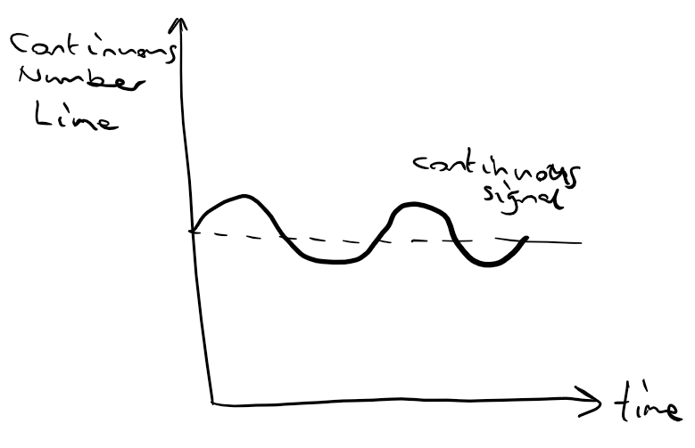
Figure 1: You can imagine a continuous signal as being perfectly smooth. There are no steps or jumps throughout its transmission.
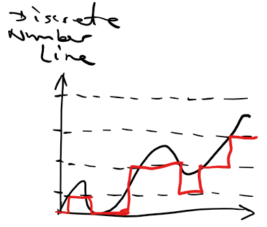
Figure 2: The red line represents the discrete signal that would be produced, by discretising this signal, in this instance. As you can see, this discrete signal consists of discrete steps. The red line is the ideal scenario, where the time to transition between states is zero. In reality, a discretised signal would have ramps at the rising and falling edges between discrete states, since it takes a small amount of time to transition from one state to another. The conversion of the black signal into the red signal is achieved through the use of a device called an Analog-to-Digital Converter, to quantise the wave at specific step values.
It is important to note that naturally, all signals are innately analogue. So, why do we design systems to take these analogue signals and make them digital? Well, by designing circuitry to control signals in a discrete manner enables a higher level of control, efficiency, reliability and precision when computing and storing information.
Digital electronic systems can process and store information much more readily, which is very useful in today’s modern digital computers. Also, compared with analogue systems, digital electronics systems are more immune to external noise interference during transmission, that might be experienced, for example, over a communications channel.
A notable downside to digital systems is a higher power consumption.
The following types of physical devices are in fact possible.
| Type | Example |
|---|---|
| Analogue Non-Electronic Devices | Pendulum Clocks, Speedometers |
| Digital Non-Electronic Devices | The Lehmer Sieve |
| Analogue Electronic Devices | Crystal Radio Receivers |
| Digital Electronic Devices | Modern Computers (PC’s, Mobile Phones) |
The Idea and Motivation
The significance of digital circuitry motivated me to design and build an analogue circuit that is the equivalent of a digital NAND-Gate; a component designed to implement what is called Boolean Logic.
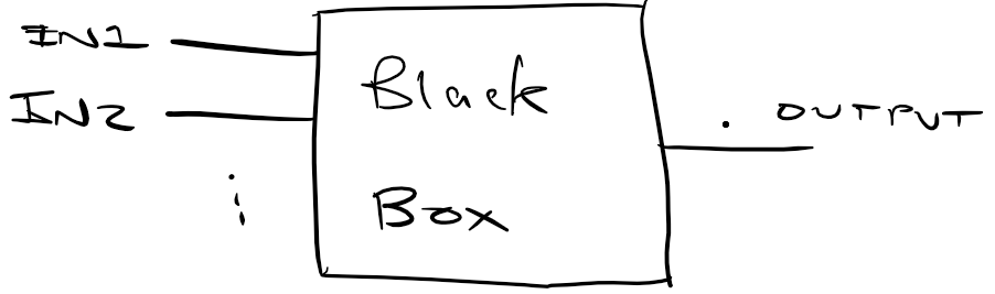
Figure 3: Imagine we have a black box, containing the necessary circuitry to represent a logic gate that obeys Boolean AND logic. There are two or more inputs and a single output. For the output to trigger HIGH/ON, all inputs must also be HIGH/ON. If any input is LOW/OFF, the output will also be LOW/OFF. The inverse conditions are true for a NAND gate, or a NOT-AND gate, where NOT outputs the inverse of the corresponding input.
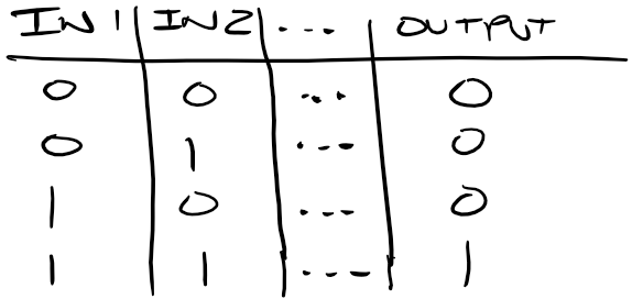
Figure 4: A table such as this one is called a truth table. A mathematical logic table relating the inputs to a logical system with the output. This is the truth table for a general NAND gate.
The physical NAND-Gate designed in this project, is a Resistor-Transistor logic (RTL) configuration, using transistors as switches and resistors to regulate voltage and current levels at points in the circuit, to agree with the electronic requirements of the two transistors - our inputs - and Light-Emitting Diode (LED) - our output.
A brief note on AC-driven electronic systems
Since we are working with a purely DC voltage source, the complexity of the physical system is greatly reduced. We need not worry about parasitic capacitances, transconductance or similar. Also, we are using the transistors as asynchronous switches, therefore we are not necessarily concerned about performance, as we would if we were designing a voltage amplifier, where precision is essential, or working with high-speed compute, where rapid transistor switching and optimal timing is required.
When dealing with AC electricity, we would refer to the resistance in terms of what is called impedence. Impedence is the effective resistance resulting in an AC-driven environment.
Impedence is mathematically represented as a vector, containing magnitude, which is the resistance caused by the DC offset in the electronic system, and a phase, known as the reactance. Reactance can be thought of as an opposition to a change in current or voltage, which occurs when an AC signal is transmitted through an electronic system.
In this design, these extra details are removed through the use of a DC voltage supply.
The benefit of using AC electricity is that an AC voltage can be much more efficiently amplified compared with a DC voltage source. However, we are working with a small electronic system over a very small distance range, and therefore do not require an AC supply.
In fact, the power supply unit in your PC converts the AC mains electricity from your mains supply to DC power supply, used to power your PC.
Before we delve into the specifics of the NAND-gate design, let’s first explore the internals of one type of transistor to gain a deeper understanding into how it is able to behave as a switch, which will provide us with a foundation for creating an Analogue system that operates under Boolean logic.
Transistor Internals 101 - Small but MIGHTY!

Figure 5: Source
The name transistor is a portmanteau of the words transfer and resistor, so transistor etymologically means transfer resistor. Resistance isn’t physically transferred by a transistor, but, due to the transistor’s physical properties, there is a relative difference between the input resistance and the output resistance. The is due to the physical make-up of a transistor, and is what enables the transistor to amplify voltages. We will explore this make-up shortly.
The transistor is well known for being the catalyst of the Information Age. It’s most common use is as an electronic switch in today’s computers, a small but mighty switch that can toggle at exceptionally high rates, while being manufactured at a size, on the low-end of the nano-scale.
There are two sole applications for the transistor.
| Function | Application |
|---|---|
| As a switch | Automated switching, at high toggle rates, makes this very useful in, for example, the control of a DC motor, high-power conversion efficiency and high switch speeds in lower-power components, such as logic gates, which we are looking at in this article. Here is an interesting discussion on what affects the switching rates of transistors. |
| As voltage amplifier | Very useful in communications for amplifying signals for transmission (think of the transceiver, and in today’s communications, optoelectrical systems). |
Types of Transistor
Several transistor designs have emerged since its physical invention in 1947. Here is a useful link on the different types of transistor. MOSFET transistors are currently the most widely used, and are the most commonly used type in microprocessors to date.
The NAND-gate circuit built in this article uses the BC548 Bipolar-Junction Transistor. Click here to read more about the uses and benefits of implement Bipolar-Junction Transistors.
The material that makes the transistor a possibility in this Universe
A semiconductor is a material whose chemical composition is such that it has an electrical conductivity that is between the range of an insulator such as hard rubber (10^-14 S/m), and a conductor such as copper (~5.96x10^7 S/m).
So how do metals and semiconductors differ structurally on a molecular scale? First, you can visualise a metal as a lattice of bonded metallic cations (positively charged ions), surrounded by a sea of negatively charged electrons. A semiconductor can also be visualised as a lattice of atoms, but this time with bound electrons and a proportion of these atoms either hold one less or one more electron in their atomic structure, leaving a gap in their regular arrangement. These gaps are known as holes, and are regarded as having a positive relative electric charge, opposite to that of the electron.
With a sufficient potential difference across a semiconductor, electrons will jump between atoms by occupying these holes, enabling a flow of current through the material and exhibiting conductive properties. There is a threshold voltage that must be met to provide the electrons with enough impetus to enable to jumps between these holes, leading to a flow of current.
The NP Junction Semiconductor
An N-type semiconductor material has a dominance of electrons in its structure, while a P-type material has a dominance of holes in its structure.
Imagine a segment of N-Type and a segment of P-Type seamlessly connected like so:

Figure 6
Opposite charges attract and like charges repel. Therefore, if we place a voltage source across the NP-junction like so:
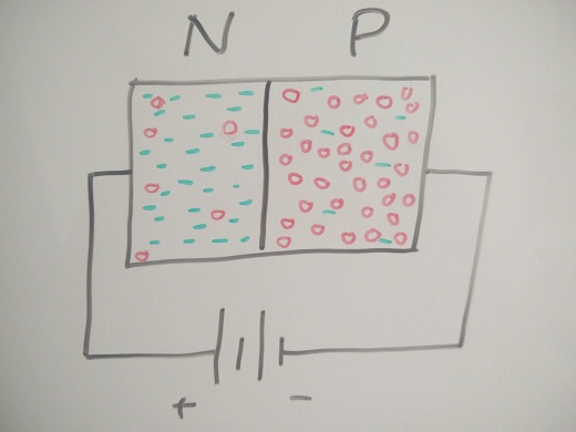
Figure 7
Then provided we have a sufficient voltage across our NP-junction, a conventional current will flow in the clockwise direction. Conventional current is a standard that refers to current as flowing from positive to negative. This is the opposite the the flow of electrons which is from negative to positive. In the proceeding sections we will be refering to conventional current.
| Type | Direction |
|---|---|
| Conventional current | + to - |
| Flow of electrons | - to + |
This circuit is the equivalent of a diode in the forward bias configuration. The threshold voltage for a diode is typically in the region of [0.6, 0.7] V.
Observing the above NP semiconductor arrangement, the polarity of the NP material provides a polarity in net charge and so a current will successfully flow through the material, with a sufficient potential difference across it. Hence the semi-conductor will begin to conduct.
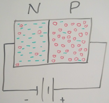
Figure 8
With the diode in reverse bias, something interesting happens. Observing the arragement above, electrons will be flowing in the clockwise direction. Therefore, electrons will be driven towards the N-Type material, while holes while flow towards the P-Type material.
At the interface between the two semiconductor regions - known as the NP-Junction - a cloud of holes and electrons forms, as electrons from the left side are forced into the P-Type holes, and holes from the right side are forced to form in the N-Type material.
Heat is produced, and breakdown of the material takes place, as shown in the depiction below. This cloud of holes and electrons shaded in the diagram, is known as the depletion region, and is the breakdown of both semiconductor devices.
When this breakdown takes place, the diode will heat up, and depending on the voltage applied across the diode in reverse bias, the diode may explode due to the rate of depletion, resulting in rapid heating and expansion.
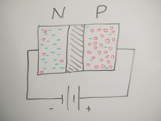
Figure 9
The NPN sandwich - Back-To-Back diodes
This brings us onto the internals of the Bipolar-Junction-Transistor.
Take our NP segment from the last section, and now sandwich the P-Type segment with a second N-Type segment. This is the equivalent of two back-to-back diodes.
Figure 10
Each segment of the NPN sandwich is controlled by a terminal like so:
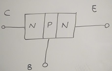
Figure 11
The Bipolar term in BJT means that there are two polarised regions in the transistor. The BJT is equivalent to two diodes, that are in series in either a back-to-back or a face-to-face arrangement. Here is a comprehensive article covering the theory behind the diode.
Why make the sandwich?
Let’s apply a voltage across our NPN sandwich like we did with the NP-segment above.
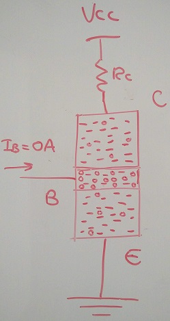
Figure 12
The resistor, Rc, is our controller for the flow of conventional current that will be driven downwards, into the upper N-Type segment of our NPN sandwich. Different BJT components have different allowed current ranges that they can safely operate with. To determine these ranges, engineers refer to datasheets.
Applying a supply voltage to the upper N-Type segment, we will find that minimal, if any, conventional current flows downwards due to there being an insufficient amount of holes occupying the lower N-Type segment.
In order for the conventional current to flow from the Vcc supply and through the NPN transistor to ground, we must apply a sufficient conventional current to the B line, known as the Base of the transistor. This increases the number of holes in the P-Type segment, promoting holes in the lower N-type segment, further polarising the NPN transistor, where it becomes more negative in the top N-Type segment.
When this happens, holes can more readily enter the upper N-Type segment from the Vcc supply, and since there will be an abundance of holes now in the lower N-Type segment, the result is an amplified net current flowing from Vcc to ground.
This is kind of like building up electrical momentum in the downwards direction, and is equivalent to closing a manual electrical switch.
Characteristically, only a small conventional current at the base is required to achieve a significantly larger conventional current through the NPN transistor.
The transistor we use in this design is the BC548 transistor, manufactured by Fairchild Semiconductor International.
Why not just use a switch? Why do we need a transistor?
Everything that a transistor can do - namely voltage amplification and switching - is entirely possible to achieve with other components. The transistor has the advantage of being able to do the same things quicker, while being smaller in size, enabling more computation, with lower power comsumption per component - like we see in today’s computers - and this can all be achieved at a much higher precision than if we did the same task mechanically.
Modeling the NAND-Gate circuit
So now that we understand how we can use a BJT as an electronic switch, let’s now devise a model for our logical NAND-gate circuit.
Below are a set of visual depictions to describe the logical function of the transistor arrangement proposed. Two BJTs are connected in series, with the collector of the upper transistor connected to Vcc and the emitter of the lower transistor connected to ground.
The red circles represent holes, while the green dashes represent electrons.
| Terminal Name | Short-hand |
|---|---|
| Base | B |
| Collector | C |
| Emitter | E |
The design in this article is for a 2-input 1-output NAND-gate. Therefore, we require two switches for the inputs to represent the HIGH/ON and LOW/OFF states. In order to control our transistor switches, we must supply their Base terminals with a current source. The way we do this here is by connecting the Base terminals to their own resistors of which are connected to the supply voltage.
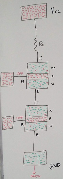
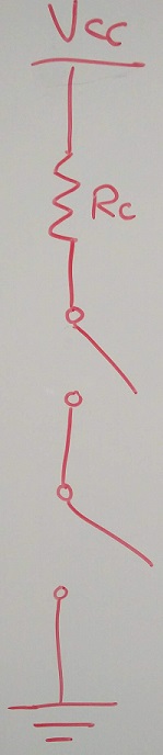
Figure 13: Imagine that each part of this design is contained in a set of black boxes. We are familiar with the NPN transistors shown. Vcc can be visualised as a box of holes, and ground as a box of electrons. We are going to be connecting the base terminals of both transistors to Vcc, seperated by current controlling resistors. Therefore, we connect each base with a box containing holes.The labels ON and OFF indicate whether or not we are supplying holes to the base of either transistor. This is the first of four possible logic states. We are supplying neither base of our transistors with a conventional current, therefore no current flows through either NPN transistor.
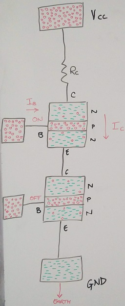
Figure 14: In this state, the upper NPN transistor is switched on, the switch is effectively closed. Current is supplied to its base, polarising the NPN transistor, by making the lower N-Type segment more positive. Therefore, conventional current passess successfully through the upper NPN transistor. However, no current is being supplied to the base of the lower NPN transistor. Therefore, its lower N-Type segment unchanged. The conventional current from the upper transistor adds holes to the lower transistor’s upper N-Type segment, however, this does not add to the downward electrical momentum we require to make the lower transistor a closed switch.
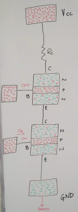
Figure 15: In this state, we are supplying the base of the lower NPN transistor with a conventional current. Since the upper transistor is an open switch, it is almost like have a ground at both N-Type segments of the lower NPN transistor. Therefore, there is no net downward conventional current.
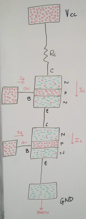
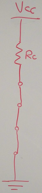
Figure 16: In this final state, both NPN transistors are closed, switches. Both are receiving a conventional current to their base terminals. Polarisation takes place in both transistors, and an overall downward conventional current results.
Now to complete our design, we add in our current controlling resistors between our supply voltage and the switches to the base of each transistor, and finally, connect an LED in parallel with the two transistors in series to display the logical output when testing.
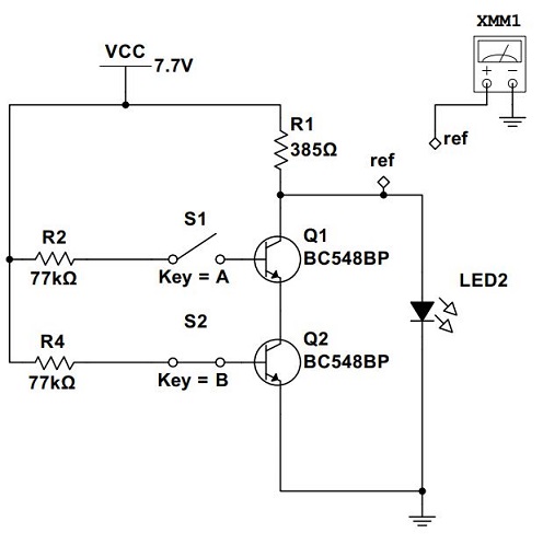
Figure 17: An NI Multisim schematic of the final BJT NAND-Gate design. Notice that the LED has been connected from the Rc transistor to ground. If we connected the transistor in series below to lower transistor, we would have an AND-Gate.
| Design Process Followed |
|---|
| Theory |
| Modeling the Circuit with different designs possibilities on a White-Board from fist principles |
| NI Multisim model with simulations to optimise design (Unit testing) |
| Physical build of circuit and Test (Testing circuit in stages at each stage of the build process) - what are the sub-systems of the circuit? |
The logical output seen with the LED:
| Lower BJT Input | Upper BJT Input | LED Output |
|---|---|---|
| OFF | OFF | ON |
| OFF | ON | OFF |
| ON | OFF | OFF |
| ON | ON | OFF |
Before the final design
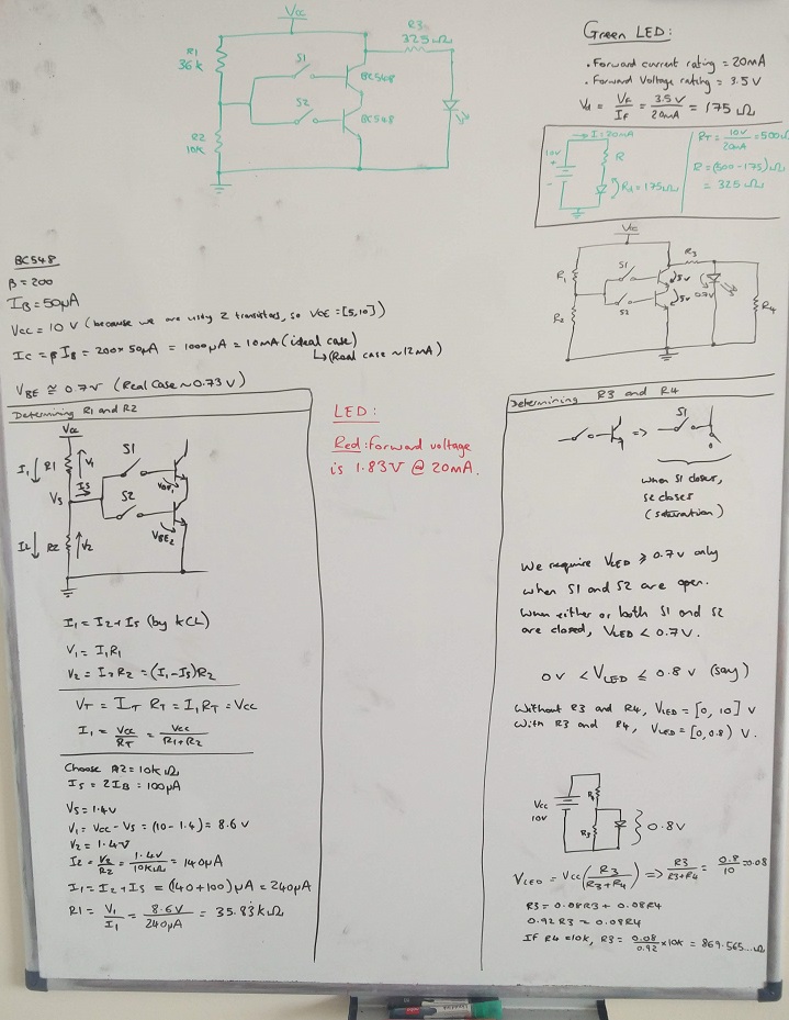
Figure 18: Here is a whiteboard working, before optimising the design to its final form.
Physical Breadboard NAND-Gate circuit
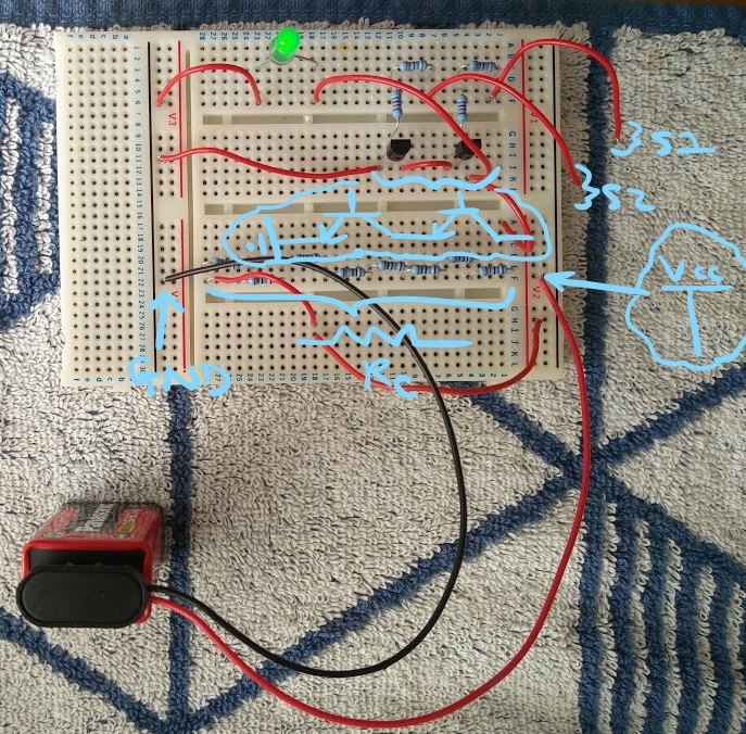
Figure 19: Here is the final physical implementation. The Vcc supply rail in shown to the right. To control the supply of current to the base of each transistor, a wire is allocated to the base of each transistor, labeled S1 and S2. The resistor pairs in series with these wires sum to 77k ohms each. At the center of this figure you can see a series of eight resistors which sum to 385 ohms, one side connected to Vcc, and the other side connected to the collector terminal of the right-most transistor. Finally, the green LED is connected in parallel with the transistors. Its cathode between Rc and the collector or the right-most transistor, and its anode connected straight to ground.